

MOSFET: The Tiny Switch That Powers Your World!
Images
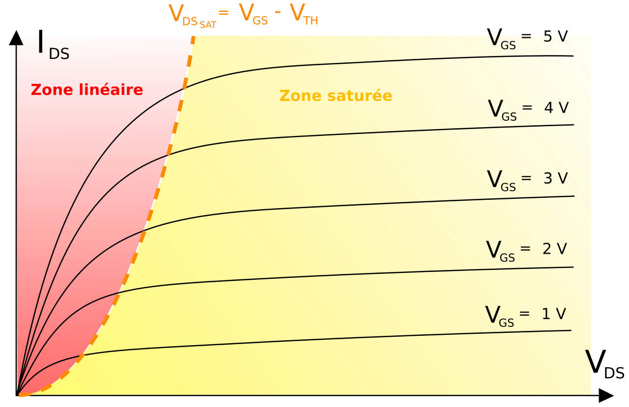
Caracteristique MOSFET


The Genesis and Evolution of the MOSFET
The MOSFET, or Metal-Oxide-Semiconductor Field-Effect Transistor, represents a pivotal advancement in semiconductor technology, fundamentally reshaping the landscape of electronics. Its conceptual roots trace back to the early 20th century, with theoretical work on field-effect devices. However, practical realization faced significant hurdles, primarily related to achieving reliable gate insulation and controlling surface states.
The breakthrough came with the development of techniques for controlled oxidation of silicon, enabling the creation of a stable and effective insulating layer (typically silicon dioxide) between the gate electrode and the semiconductor channel. This innovation, largely credited to scientists at Bell Labs and other research institutions in the mid-20th century, overcame the limitations of earlier transistor designs. The ability to fabricate these devices using established silicon processing techniques, coupled with their inherent low power consumption and scalability, positioned the MOSFET as the dominant transistor type for integrated circuits, driving the digital revolution.
Unpacking the Electrophysics
At its core, the MOSFET operates on the principle of modulating the conductivity of a semiconductor channel through an applied electric field. The device typically consists of a semiconductor substrate (often silicon) with two highly doped regions forming the source and drain terminals. Between these is a channel region whose conductivity is controlled by a gate electrode, separated from the substrate by a thin dielectric layer (the 'oxide').
When a voltage is applied to the gate, it induces charge carriers in the semiconductor region beneath the dielectric. For an enhancement-mode n-channel MOSFET, a positive gate voltage attracts electrons, forming an 'n-type' inversion layer that connects the source and drain, allowing current to flow. Conversely, a negative gate voltage depletes these carriers, increasing the channel's resistance.
The 'metal' in the name is often a historical artifact, as polysilicon gates are now prevalent, and alternative high-k dielectric materials are used to enhance performance and reduce gate leakage current. This voltage-controlled behavior, requiring minimal gate current under DC conditions, is a key advantage.
The Indispensable Role of MOSFETs in Modern Technology
The significance of the MOSFET cannot be overstated; it is the foundational element of virtually all modern digital electronics. Its scalability, low static power consumption, and high switching speeds have enabled the creation of complex integrated circuits (ICs) containing billions of transistors on a single chip. This miniaturization is the driving force behind the exponential growth in computing power described by Moore's Law.
MOSFETs are the workhorses in microprocessors, memory chips (DRAM and flash), logic gates, and digital signal processors. Complementary Metal-Oxide-Semiconductor (CMOS) technology, which utilizes pairs of n-type and p-type MOSFETs, offers extremely low power dissipation during operation, making it ideal for battery-powered devices like smartphones and laptops. Beyond digital applications, MOSFETs are also employed in power electronics for efficient switching and voltage regulation in everything from power supplies to electric vehicles.
Design Variations and Performance Enhancements
While the basic MOSFET structure is well-defined, numerous design variations and enhancements exist to optimize performance for specific applications. Enhancement-mode MOSFETs, which are normally 'off' and require a gate voltage to turn 'on', are the most common type for digital logic. Depletion-mode MOSFETs, conversely, are normally 'on' and require a gate voltage to turn 'off'.
Further refinements include the development of different channel types (n-channel and p-channel), which can be combined in CMOS logic for superior efficiency. Advanced fabrication techniques have led to smaller feature sizes, increased speed, and reduced power consumption. Innovations like FinFETs (Fin Field-Effect Transistors) and Gate-All-Around (GAA) transistors represent architectural shifts designed to overcome the physical limitations of planar MOSFET scaling, maintaining electrostatic control over the channel as dimensions shrink further.
These ongoing developments ensure the MOSFET's continued relevance in the face of ever-increasing performance demands.
From Foundational Science to Future Frontiers
The MOSFET's journey from a laboratory curiosity to the bedrock of the digital age is a testament to relentless innovation in materials science and electrical engineering. Its ability to act as a highly efficient, voltage-controlled switch has enabled the miniaturization and proliferation of electronic devices that define modern life. As technology pushes the boundaries of physics, research continues into novel materials and device architectures beyond traditional silicon MOSFETs.
Exploring new dielectrics, channel materials, and three-dimensional structures aims to overcome fundamental scaling limits and unlock new functionalities. The principles pioneered by the MOSFET continue to inspire the development of next-generation semiconductor devices, promising even more powerful and efficient electronics for the future, potentially impacting areas like artificial intelligence, quantum computing, and advanced sensing technologies.
See also
Frequently Asked Questions
What is a MOSFET and why is it called a tiny switch?+
How does a MOSFET let electricity flow or stop?+
Why do MOSFETs use a thin layer of silicon dioxide?+
How did scientists make MOSFETs small and efficient?+
Where can we find MOSFETs in everyday gadgets?+
Based on content from Wikipedia · Licensed under CC BY-SA 4.0